

The JSM-7001F analytical thermal field emission SEM is the ideal platform for demanding analytical applications as well as those requiring high resolution and ease-of-use. The JSM-7001F has a large, 5-axis, fully eccentric, motorized, automated specimen stage, a one-action specimen exchange airlock, small probe diameter even at large probe current and low voltage, and expandability with ideal geometry for EDS, WDS, EBSP, and CL. The specimen chamber handles specimens up to 200mm in diameter.
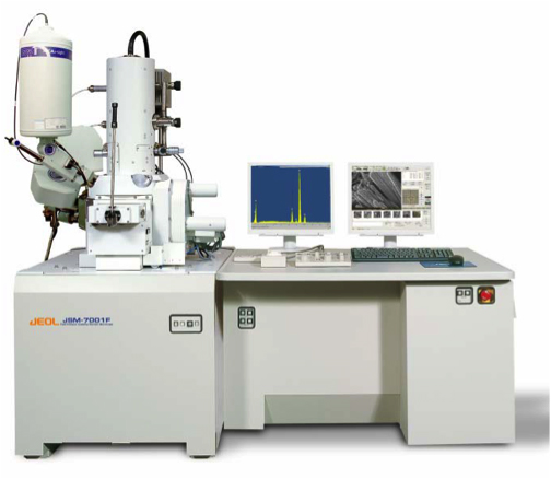
JSM-7001F Key Product Features
Resolution
(secondary electron image)
1.2 nm (at 30 kV)
3.0 nm (at 1.0 kV)
3.0 nm (at 15 kV 10mm WD, 5nA)
Accelerating Voltage
0.5 to 2.9 kV (10V steps)
3.0 to 30 kV (100V steps)
Magnification
x10 to 1,000,000x (printed as a 120mm x 90mm micrograph)
Imaging Modes
SEI (secondary electron image)
BEI to E/T Detector
BEI - Option (backscattered electron image TOPO and COMPO
Resolution
(secondary electron image)
- 1.2 nm (at 30 kV)
- 3.0 nm (at 1.0 kV)
- 3.0 nm (at 15 kV 10mm WD, 5nA)
Accelerating Voltage
- 0.5 to 2.9 kV (10V steps)
- 3.0 to 30 kV (100V steps)
Magnification
- x10 to 1,000,000x (printed as a 120mm x 90mm micrograph)
Imaging Modes
- SEI (secondary electron image)
- BEI to E/T Detector
- BEI - Option (backscattered electron image TOPO and COMPO)